CIQTEK EPR
Centro prodotti

Prodotti

Scienza e tecnologia quantistica
La tecnologia quantistica appartiene al campo strategico e fondamentale dell’innovazione scientifica e tecnologica di frontiera, che può superare il collo di bottiglia della tecnologia classica aumentando la velocità di calcolo, migliorando l’accuratezza della misurazione e garantendo la sicurezza delle informazioni.
Scienza dei materiali
Utilizzando strumenti analitici avanzati, studia l'interrelazione tra il processo di preparazione o lavorazione dei materiali, la microstruttura dei materiali e le proprietà macroscopiche dei materiali.
Sostanze chimiche
Sostanze chimiche
L'analisi della struttura di sostanze contenenti elettroni spaiati (come singoli atomi isolati, conduttori, molecole magnetiche, ioni di metalli di transizione, ioni di terre rare, cluster di ioni, materiali drogati, materiali difettosi, radicali biologici, metalloproteine, ecc.) e le loro applicazioni sono realizzato mediante la spettroscopia d’onda.
Scienze industriali e applicate
Fornire prodotti e soluzioni di alta qualità e standard elevati per gli utenti industriali e la ricerca scientifica applicata basata su tecnologia avanzata e prodotti affidabili.
Energia e potenza
Energia e potenza
Concentrarsi sull'utilizzo di risorse di petrolio e gas non convenzionali come petrolio e gas di scisto, metano da carbone, ghiaccio combustibile, ecc. e sviluppare scenari applicativi come il rilevamento quantistico del fondo pozzo e l'analisi del nucleo digitale.
Biomedica e scienze della vita
Applicare per risolvere la struttura e la funzione delle macromolecole biologiche, dell'imaging di singole molecole, dell'imaging subcellulare, dello smistamento cellulare e di altri campi, la scala di misurazione spazia dal nanometro alla scala del micron.

Informazioni su CIQTEK

CIQTEK è lo sviluppatore e produttore globale di strumenti scientifici di alto valore. La nostra attività principale include microscopi elettronici (SEM/FIB, TEM), spettrometri a risonanza magnetica nucleare (NMR), spettrometri a risonanza paramagnetica elettronica (risonanza di spin elettronico) e analizzatori di area superficiale e pori BET.
  • 0+
    Dipendenti
  • 0% +
    Dipendenti dedicati alla ricerca e sviluppo
  • 0+
    Brevetti in attesa o concessi
Notizie ed eventi

Notizia

Cosa c\'è di nuovo
CIQTEK Unveils CryoHe Probe and High-Field Solid-State NMR Systems
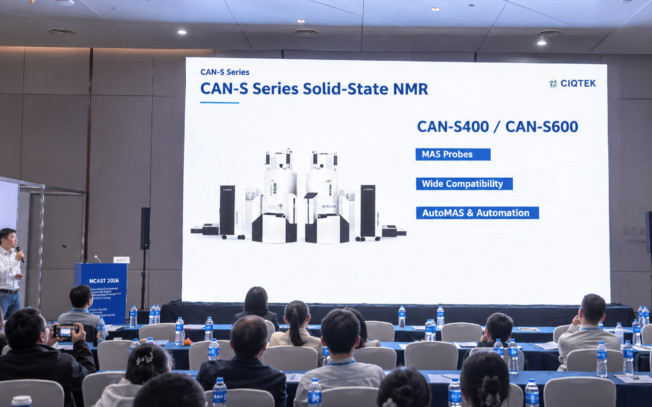
CIQTEK has expanded its NMR portfolio with two new developments: the CryoHe Series helium cryogenic NMR probe and the CAN-S400 and CAN-S600 high-field solid-state NMR spectrometers. Unveiled on October 31 during the 2nd Conference on Analytical Science and Instrumentation (NCASI 2026) in Wuhan, China, the new products address two important needs in NMR research: higher sensitivity for challenging liquid-state samples and high-field structural characterization of solid materials. Figure 1. Launch of the CIQTEK CryoHe Probe and CAN-S Solid-State NMR Systems CryoHe: Higher Sensitivity at Cryogenic Temperature In NMR spectroscopy, sensitivity can determine whether weak signals are detected at all, especially when working with low-concentration, low-abundance, or compositionally complex samples. The CIQTEK CryoHe Series helium cryogenic probe uses closed-cycle deep cryogenic cooling to stabilize the core RF coil at around 20 K. Compared with a conventional room-temperature probe, the CryoHe probe can typically improve the signal-to-noise ratio by around 2× or more for nuclei such as ¹H and ¹³C. When the same signal-to-noise level is required, this can shorten measurement time by roughly an order of magnitude. The probe supports ¹H, ¹³C, ¹⁵N, ³¹P, and ¹⁹F, together with automatic tuning and matching. A low-temperature ²H preamplifier is used to improve lock signal quality and magnetic-field stability. These capabilities are particularly useful in areas such as structural biology, drug research, metabolomics, and natural product analysis, where samples may be limited in quantity or difficult to characterize using conventional sensitivity levels. Figure 2. CIQTEK CryoHe Cryogenic Probe with a 600 MHz Liquid-State NMR System CAN-S400 and CAN-S600 for High-Field Solid-State NMR CIQTEK also introduced the CAN-S400 and CAN-S600 high-field solid-state NMR spectrometers, extending the CAN platform into solid-state NMR applications. Solid-state NMR enables researchers to study the chemical environment and molecular dynamics of insoluble or poorly soluble solid materials while preserving their structure. The CAN-S Series uses a distributed spectrometer architecture and high-uniformity, high-stability superconducting magnets, with 9.4 T and 14.1 T configurations currently supported. Multiple rotor sizes are available, including 3.2 mm, 4 mm, and 7 mm. The 3.2 mm rotor supports spinning speeds of up to 24 kHz. The system supports automatic magic-angle calibration, probe tuning and matching, as well as MAS speed setting and monitoring, rotation stability control, gas-path status monitoring, and abnormal-condition protection. At the hardware level, the CAN-S platform uses an integrated architecture that also supports liquid-state NMR workflows, allowing more efficient switching between solid-state and liquid-state measurements within the broader CAN platform.   Expanding the CIQTEK NMR Platform The si...
November 13, 2026
From Imaging to Reports: CIQTEK Launches SEM Agent
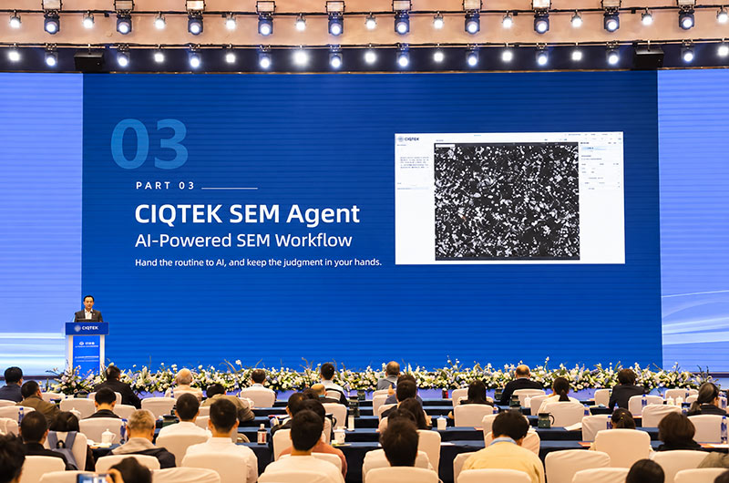
What if you could simply tell your SEM what you need, then let it handle the repetitive work? CIQTEK has launched SEM Agent, an AI-assisted platform designed to connect SEM imaging, analysis, and reporting in one workflow. Users can describe a task by text or voice, and the system can call more than 40 tools to carry out steps from area selection and image acquisition to data analysis and report generation. The idea is simple: reduce the time spent adjusting settings, searching for areas of interest, moving data between software, and organizing reports, while keeping the researcher in control of the final scientific judgment. Figure 1. CIQTEK SEM Agent Unveiled at the 2026 Electron Microscopy Conference Why SEM Workflows Need More Than Better Hardware A powerful microscope does not automatically mean a more efficient workflow. In everyday SEM work, researchers may still spend a large amount of time adjusting parameters, locating samples, organizing images, moving results between different software tools, and preparing reports. Many successful methods also remain tied to individual experience. When a new sample or task appears, the workflow often has to be rebuilt or adjusted manually. SEM Agent is designed to connect the microscope, analysis tools, and workflow knowledge around the task the user actually wants to complete. One Request, One Connected SEM Workflow Instead of operating each step separately, users can describe the task they want to complete. For example, a user can ask SEM Agent to image a lithium iron phosphate sample from 2,000× to 100,000× magnification, organize the images, analyze the results, and prepare a sample report. The system can then check microscope status and imaging conditions, adjust brightness, focus and stigmation, switch between magnifications, collect images, evaluate image quality, analyze sample features, save the results, and organize them into a report. Figure 2. Automated Multi-Magnification Imaging of a Lithium Iron Phosphate Sample Large-area acquisition is another typical task. In one chip demonstration, SEM Agent collected 70 fields of view in a 7 × 10 grid at 1,000× magnification and stitched the images into a larger overview. Each local image remained traceable to its original position. This helps reduce repetitive stage movement and the time normally spent sorting and organizing images after acquisition. Figure 3. Large-Area Automated Acquisition and Image Stitching Image Analysis Built Around the Sample SEM Agent is not limited to image acquisition. Users can also describe what they want to measure or identify, and the system can organize the corresponding analysis workflow. Current applications include particle size analysis, diamond wire measurement, nickel layer inspection, and defect analysis. Depending on the task, the workflow can include segmentation, measurement, statistics, and visualization. The goal is to reduce repetitive manual tracing, counting, and result organi...
November 02, 2026
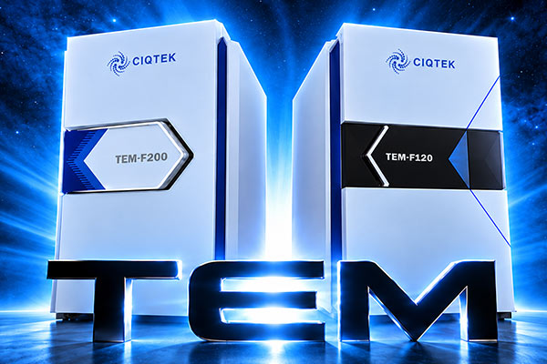
CIQTEK Unveils TEM-F200: 200 kV Field Emission TEM
CIQTEK has officially launched its 200 kV field emission transmission electron microscope, TEM-F200, delivering 0.10 nm information resolution and featuring several key subsystems developed in-house. Unveiled on October 18 at the 2026 National Electron Microscopy Annual Conference in China, the TEM-F200 is designed for demanding work in materials science, semiconductor research, and nanoscale characterization. The launch also marks another step toward a more complete domestic TEM platform, from key hardware to imaging and analysis workflows. Built Around Resolution, Stability, and Practical Use For TEM users, resolution is only part of the story. Stability, ease of operation, detector performance, automation, and service all affect what the microscope can actually deliver day-to-day. The TEM-F200 combines a 200 kV field emission electron source with a self-developed high-voltage power supply and optical system. TEM-F200 Key Specifications 200 kV Field Emission Transmission Electron Microscope Acceleration Voltage 20 to 200 kV Information Resolution 0.10 nm Point Resolution 0.25 nm STEM Resolution 0.16 nm STEM Detector Modes HAADF, ADF, ABF Magnification 20× to 1,200,000× Super-EDS Optional dual 100 mm² windowless SDD detectors with symmetrical geometry, energy resolution ≤127 eV Optional Configurations EELS, 4D-STEM, 3D-ED, in situ sample holder A thermostatic water-cooled objective lens and four-axis sample stage help support stable imaging, while automated aperture control, position memory, and one-click adjustment are designed to reduce repetitive manual work. The main imaging camera is CIQTEK’s self-developed 16-megapixel fiber-coupled CMOS camera, built specifically for TEM use. The camera combines a 9 μm CMOS sensor, 4K × 4K imaging, and up to 24 fps at full resolution. Less Time at the Controls, More Time on the Sample The TEM-F200 also puts a strong focus on workflow. Fluorescent-screen images can be transferred directly to the PC display, while high-voltage control, electron-gun auto-start, vacuum operation, sample-position auto navigation, and STEM detector movement can all be integrated into the system workflow. For laboratories that need more flexibility, the platform can also be expanded with EDS, EELS, 4D-STEM, 3D electron diffraction, side cameras, cryogenic components, and in situ holders. From FinFET Devices to Advanced Alloys The new system has already been demonstrated on a range of demanding samples. For semiconductor FinFET devices, local nanoscale features and fine lattice structures were clearly resolved, with FFT analysis showing a spacing down to 1.045 Å. Semiconductor FinFET Cross-sectional imaging of semiconductor memory chips clearly revealed multilayer thin-film and dielectric structures. For 7075 aerospace aluminum alloy, TEM-BF and STEM-HAADF imaging resolved nanoscale precipitates, discontinuous grain-boundary phases, and precipitate-free zones. The system was also used to e...
October 26, 2026
Conferenze e mostre
CONTATTACI

Contatto

Superiore

Lasciate un messaggio

Lasciate un messaggio
Non esitate a contattarci per maggiori dettagli, richiedere un preventivo o prenotare una demo online! Ti risponderemo il prima possibile.
Invia

Casa

Prodotti

Chiacchierata

contatto