Che cosa sta cercando?
Ricerche popolari
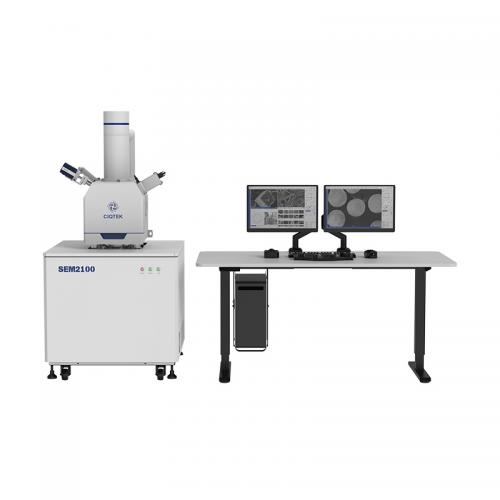
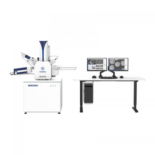
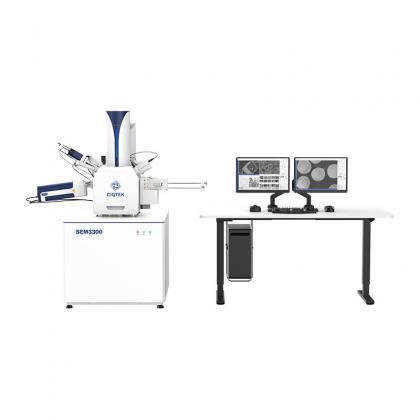
- Fornitore globale del produttore di microscopi elettronici a scansione a emissione di campo
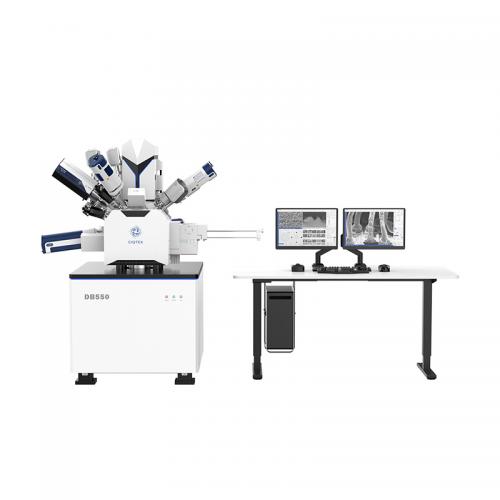
- Rivelatori SEM EDX, EDS, EBSD, BSE, CL, STEM
- Applicazioni QDAFM del magnetometro NV a scansione del microscopio a forza atomica a diamante quantistico
- Produttore di microscopi per centri NV con scansione ciqtek
- Fornitore globale di magnetometria NV di scansione
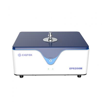
- Fornitore globale di spettroscopia di risonanza paramagnetica elettronica a impulsi in banda X
- Spettroscopia di risonanza paramagnetica elettronica Miglior prezzo
- Spettroscopia EPR in banda X con criostato
- Spettroscopia di risonanza paramagnetica elettronica in banda W Miglior prezzo
- Spettroscopia di risonanza di spin elettronica in banda W Miglior prezzo